During a recent shopping mania I grabbed some old AMOLED screens at very cheap price. The seller is an electronics hobbyist. He is kind enough to provide an adaptor board that generates required bias voltages for the screen. Unfortunately the board uses 2×12 DIL header, pain in the arse for breadboarding. I realize this is a perfect opportunity to test drive my MF70 CNC for PCB milling. So I quickly fire up Eagle and create a DIL to DIP adaptor.

To produce the necessary G-code I use Seeedstudio Fusion PCB service CAM script to create Protel compatible Gerber files for bottom layer and drill data, then load the Gerber in CopperCam. (Tip: In CopperCAM, turn off Parameters->Automatic Alignment to have drilling holes proper aligned manually).

The tools I choose is 0.1mm, 30° engraving bit for isolating, 0.9mm drill bit for the holes and 1.5mm endmill for outline cutting. The cutting depth for isolating path is set to 0.1mm. I choose not to hatch out the excessive cooper as I plan to peel them off manually.
The flatness of board is critical in PCB milling. I use a 5mm acrylic board as the “sacrifice” base and double side tape a blank PCB on top of it. Double side tape appears to be pretty handy here because otherwise when the board is clamped down at both sides, the centre part tends to bend upwards.

Since the cutting depth is only 0.1mm, an absolutely accurate zero in Z axis is crucial. USB CNC Controller software provides a very useful function, using a tool sensor as Z- limit switch to measure Z offset. During the measurement, the spindle is moved down until the tool touches the sensor block. The software will record this point, then subtract the block height to receive Z axis zero.

As recommended by many people, drilling should be done first. This is because otherwise for small pads the high shearing force during drilling could remove the whole pad. Step 2 is mill the isolation tracks, followed by cutting out the board.
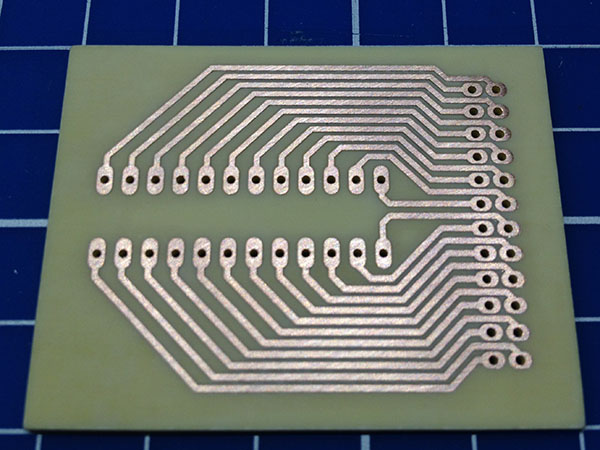
Here is the result. Looks pretty decent for first time milling. Notice the residue copper in between the tracks. I believe this is less than 10mil.

After peeling off the excessive copper, the final PCB looks great!

Final words
From young I’ve been using ferric chloride etching method to make my own PCBs. However several years ago this chemical was banned by the government here in Singapore because some irresponsible people had been pouring wastage into the drainage. The ban is reasonable. No shop sells ferric chloride any more. But under the spirit of Kiasu shop owners dare not carry other environmental friendly solutions such as Sodium Persulfate either. Ironically they do carry other etching necessities like photo sensitive PCBs and developer solutions. But who will buy these without the etchant?
Many innovations have since been killed in the infancy. While the government keeps advocating innovation and improving productivity, without a proper environment of promoting science studies, without an open community, without the courage to step forward, people will forever crawl in the cradle.
Anyway, new year, new start…
Hi,
where did you get the tool sensor for measuring z-axis offset? And what software did you use for usb cnc controller?
Best regards
Hi,
The tool sensor is from China. It is not as useful as it looks, a piece of PCB material is good enough for the job.
The software is from http://www.planet-cnc.com
Hello,
can you please tell me the USB CNC controller are you using?
Thanks,
http://www.planet-cnc.com